This article explores the importance of reducing electromagnetic interference (EMI) in PCB designs. EMI can have serious consequences for the performance and reliability of electronic systems, so understanding how to reduce it is essential for safety and quality assurance.
We will look at various strategies that designers can use to ensure their circuits comply with relevant standards while delivering the desired level of performance. Additionally, we will explore best practices when it comes to designing PCBs that are resilient against EMI.
Finally, we will discuss potential solutions for minimizing EMI in a variety of applications.
Design Considerations for Minimizing EMI
There are many design considerations and methods to reduce electromagnetic interference (EMI) when designing PCBs. Shielding, routing techniques, ferrite beads, decoupling capacitors, and proper grounding are all important elements in reducing the impact of EMI on a PCB design.
Shielding involves encasing sensitive components with metal layers that act as barriers against unwanted electrical signals from entering or leaving the board. Routing techniques focus on controlling signal paths to avoid crosstalk between circuits while also isolating high-speed signals from slower ones.
Ferrite beads can be used to absorb noise generated by switching devices such as relays and solenoids before they reach other parts of the circuit board. Decoupling capacitors placed near power sources can help filter out any sudden voltage changes that could lead to EMI generation.
Finally, proper grounding is essential since a ground plane helps dissipate static electricity away from sensitive components while also providing an ideal return path for current flow within the circuit board itself. By considering these design elements when building your next PCB project you can be sure that your product will have optimal protection against unwanted electromagnetic interference without sacrificing performance or reliability
Utilizing Shielding Techniques to Block EMI

Source: www.ultralibrarian.com
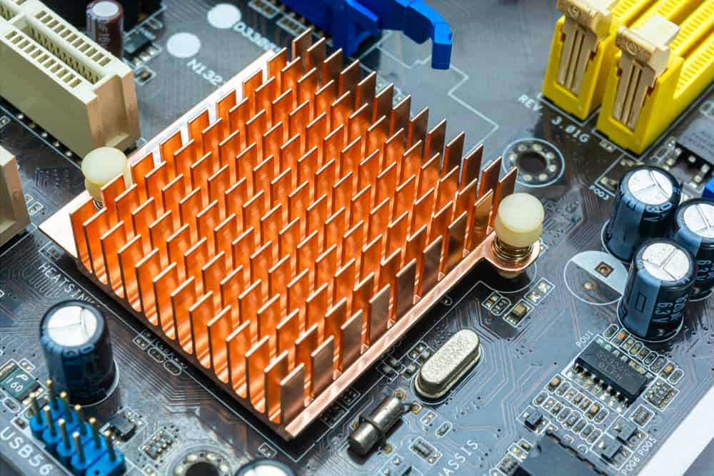
Shielding is a highly effective technique for minimizing electromagnetic interference (EMI) in PCB designs. It involves the use of conductive barriers to create an enclosed space, which helps to block the transmission of EMI between components and reduce the amount of noise that can be generated.
Shielding materials such as copper tape or metalized fabric can be used to form barriers around sensitive areas on a circuit board, or even completely enclose entire boards if necessary. These shielding techniques help minimize signal loss due to EMI and also add additional protection against external sources of EMI like radio frequency transmissions from nearby electrical devices.
Additionally, they allow designers more freedom when it comes to positioning components without worrying about crosstalk caused by physical proximity between them. When applied correctly, these shielding strategies can significantly improve the performance and reliability of PCB designs while preventing damage caused by stray signals or high-frequency radiation.
Selecting Components with Low Electromagnetic Emission Levels
When designing a PCB, reducing electromagnetic interference (EMI) is essential. Selecting components with low EMI levels and implementing appropriate shielding techniques can help minimize the risk of interference.
By choosing components that have been tested for their EMI characteristics, designers can ensure that their circuit boards are compliant with applicable standards and regulations. To determine which components best meet these requirements, it is important to consider several factors such as noise emission level, frequency range, power rating, and operating temperature.
Furthermore, some types of devices may require additional considerations due to their particular use in the system or application being designed. For instance, active electronic components like amplifiers or oscillators typically generate more emissions than passive ones like resistors or capacitors.
As such they need special attention when selecting them for a design aiming at minimizing EMI levels on the board’s interface connections. Another factor to take into account is where on the board each component will be placed; this could influence how well-shielded it might be from external sources of noise and other interferences.
In general terms, hot spots generated by high-speed integrated circuits should also be taken under consideration since these areas are particularly prone to electromagnetic radiation problems due to their higher current density levels compared with other parts of a printed circuit board assembly (PCBA). Finally, environmental conditions-related aspects must also be considered to choose properly shielded solutions capable of performing optimally within expected operational settings; while still providing adequate protection against radiated emissions coming from outside sources as well as internal sources inside the PCBA itself – including those generated during startup phases when currents may peak significantly above nominal values specified per device datasheets.
Implementing Ground Planes and Power/Ground Rails

Source: resources.altium.com
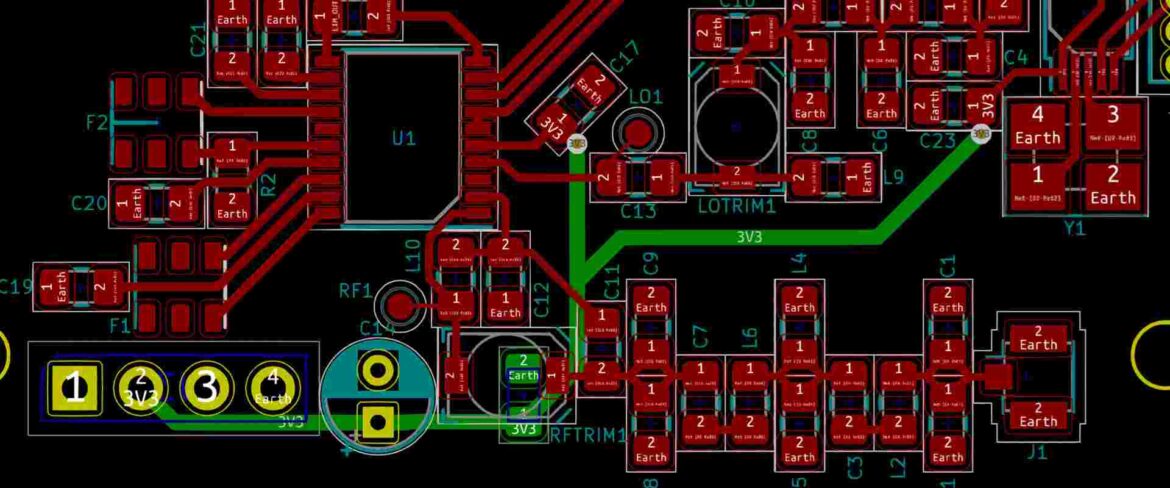
Ground planes and power/ground rails are essential components of reducing EMI in PCB designs. They help to create shielding between the circuits, providing a low-impedance path for ground currents.
To implement them effectively, designers need to understand how they interact with each other and with the surrounding circuitry. Ground planes should be used as a single, continuous layer covering all signal layers; this helps reduce the loop area that can cause interference.
Power/ground rails should be routed on multiple layers throughout the board to ensure adequate grounding connections between circuits without introducing noise or interfering signals from adjacent traces. The use of vias also helps maintain good connectivity when routing power/ground rails over long distances and across different layers of the board.
When designing ground planes and power/ground rails, it is important to keep in mind factors such as track widths, clearances between tracks, current carrying capacity requirements, etc., so that optimal performance is achieved while maintaining EMC compliance levels
Conclusion
Reducing Electromagnetic Interference (EMI) in PCB Designs is an important consideration for any product that requires reliable performance and operation. Utilizing proper shielding techniques, such as copper foils, ground planes, and vias can help to reduce the amount of EMI generated within a design.
Additionally, utilizing Flex-Rigid PCB technology can provide more robust protection against EMI while also allowing for greater flexibility in component placement. By taking the necessary steps to reduce EMI it is possible to ensure long-term reliability with products that contain printed circuit boards.
Source: resources.pcb.cadence.com

